Overview
The Thermofisher Tecnai Osiris is a modern analytical 60-200 kV scanning/transmission electron microscope (S/TEM). Its constant-current lens design delivers rapid access to high resolution TEM and STEM imaging with minimal alignments. The Osiris is equipped with an industry-leading energy dispersive X-ray spectroscopy (EDS) SuperX™ detection system, achieving highest efficiency detection of all elements down to and including boron. Drift-corrected STEM-EDS maps utilizing this system enables quantifiable chemical imaging at the nanoscale. In conjunction with the Fischione 2020 Advanced Tomography Holder, 3D TEM, STEM and STEM-EDS imaging at the nanoscale is possible. Further, structural dynamics can be visualized utilizing the in-situ heating abilities available with the use of the Protochips Aduro Platform or Gatan In-situ heating holder.
Capabilities
Imaging
- Conventional Bright-Field and Dark-Field TEM imaging at 60 kV to 200 kV
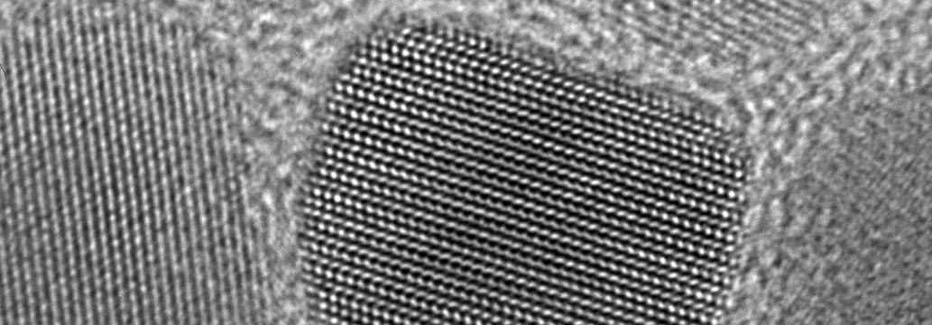
- High Resolution TEM with better than 0.2 nm resolution
- High Resolution HAADF (Z-contrast) STEM with 0.16 nm resolution
- Electron Diffraction via Selective Area Electron Diffraction or Convergent Beam Electron Diffraction
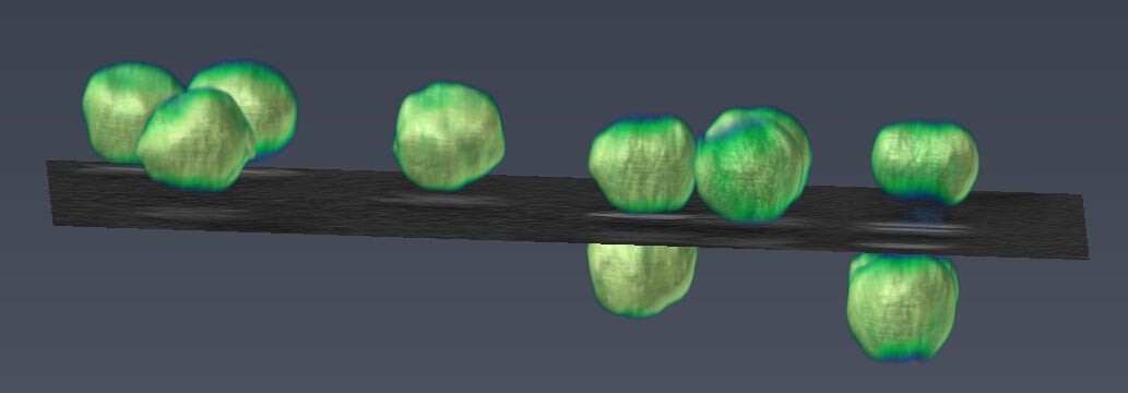
- 3D imaging of nanostructure morphology with TEM and STEM tomography
- Automated through focal series collection and exit wave reconstruction with TrueImage
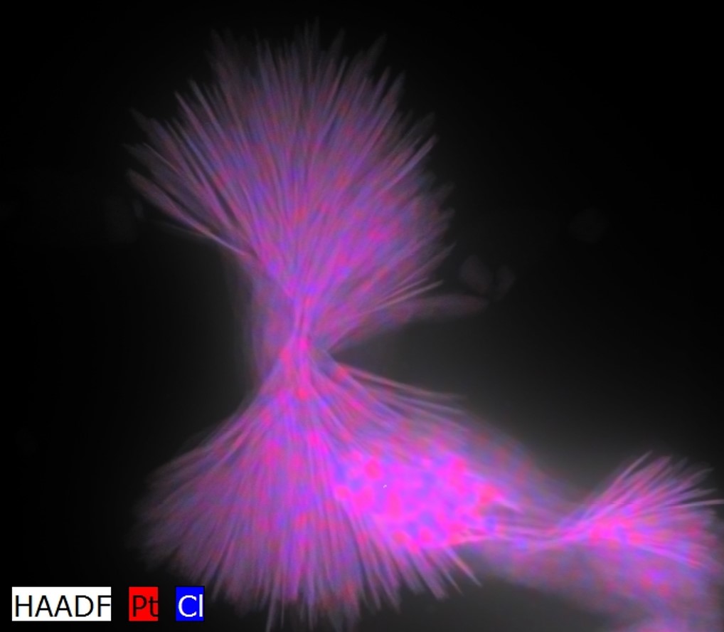
Spectroscopy - SuperX™ Empowered Energy Dispersive Spectroscopy
- TEM-EDS for element detection down to and including boron
- STEM-EDS chemical mapping with sub-nm spatial resolution
- Rapid chemical imaging with quantifiable results
- STEM-EDS in 3D with tilt-insensitive detector positions
In-Situ Heating
- Protochips Aduro Platform – room temperature to 1200 ˚C
- Gatan in situ Heating Holder – tantalum crucible for conventional TEM samples, up to 1300 ˚C
Software
- Amira 3D visualization software
- Inspect3D tomography reconstruction software
- Trueimage exit wave reconstruction software
- Bruker Esprit 1.9 EDS analysis software
Applications
- Micro to nanoscale imaging
- Particle sizing
- Negative stain
- High resolution crystal lattice imaging
- Crystal structure determination
- Nanoparticle characterization
- Chemical imaging of nanostructures and fixed biological samples
- 3D imaging of nanostructures
- In-Situ annealing
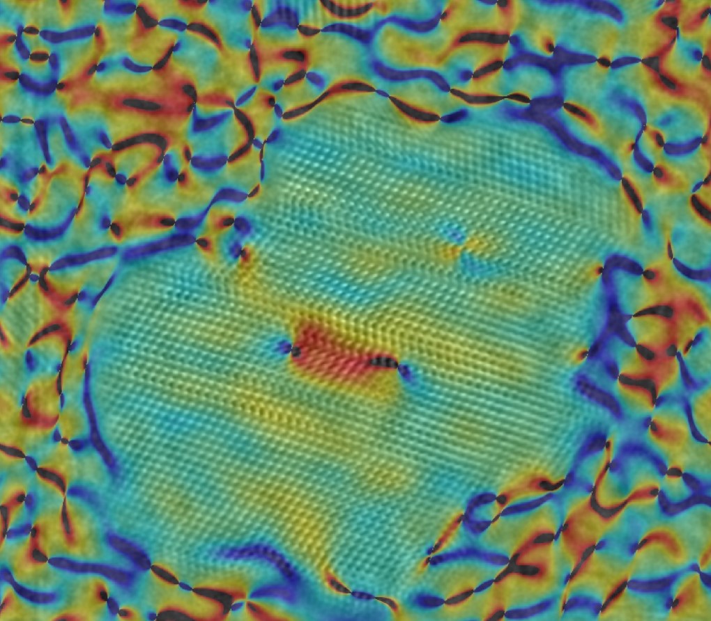
- Atomic-level strain imaging
- Defect analysis
Contact
-

Dr. James McBride
VINSE Advanced Imaging
- 011 Engineering Science Building