Overview
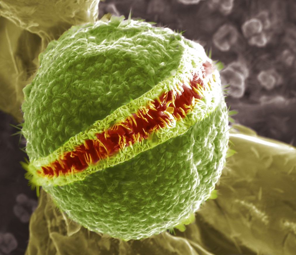
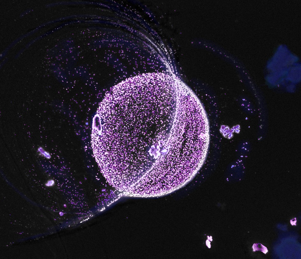
The Zeiss Merlin is a highly capable and user-friendly scanning electron microscope designed for rapid imaging of micro to nanoscale samples. The Merlin is fully equipped with all common modes of imaging, including secondary electron, backscattered electron and STEM-in-SEM. Further, chemical analysis and mapping is available with the Oxford X-max 50 SDD EDS system.
Capabilities

Imaging
- High resolution SEM for 1 kV up to 30 kV
- Everhart-Thornley secondary electron detector
- In-lens secondary and energy selective backscatter detector
- Segmented STEM detector and dedicated TEM grid holder
- 4-Quadrant backscattered electron detector
Spectroscopy
- Energy Dispersive Spectroscopy (Oxford X-MAX 50 SDD)
Charge Compensation
- Gas injection needle for charge compensation for improved imaging of non-conductive samples
Software
- Oxford Aztec 3.3 EDS Analysis Software
Applications

- Micro to nanoscale imaging
- Surface Imaging
- Fabrication process validation
- Nanoscale metrology
- Chemical analysis and mapping
- STEM in SEM imaging for low voltage transmission imaging of tissue and beam sensitive materials
- Gunshot residue (GSR) analysis
- Failure analysis
Contact
-

Dr. James McBride
VINSE Advanced Imaging
- 015 Engineering Science Building