Overview
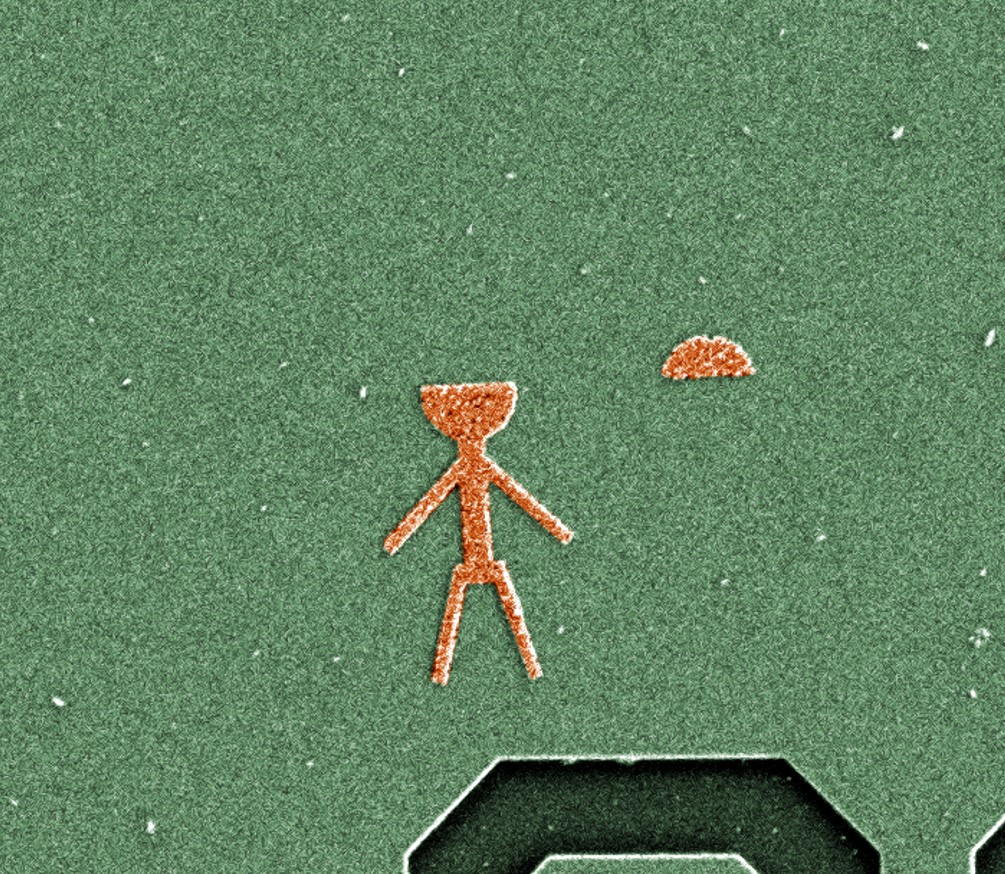
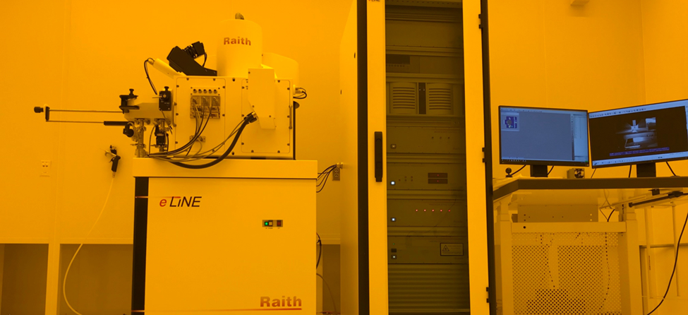
The Raith eLine Electron Beam Lithography system is a SEM0-style instrument that enables high resolution imaging and nanoscale device patterning of standard semiconductor, metal, and dielectric materials. The tool combines high performance, exceptional versatility, and ease of use for both tool and software.
Capabilities
- Emission source: thermal field-emission tungsten coated with Zirconia
- Writing current: 5 pA-20 nA
- Operating voltage: 0.1 kV to 30 kV
- Aperture sizes: 7.5, 10, 20, 30, 60, 120 μm
- Beam size: 2 nm at 20 kV at 3 mm working distance
- Detectors:
- SE2 (secondary electron detector)
- In-Lens
- Chamber optical camera
- Sample size:
- Holder has clips for up to 6 20 mm x 20 mm samples simultaneously
- Maximum sample size: 1 3 inch diameter wafer
- Maximum sample height: <11 mm
- Write field size: 5 μm to 2 mm
- Precision stage controller
- Minimum feature size: < 20 nm dependant on column parameters, sample and resist type
- Airlock for quick sample exchange (~8 minutes)
- High Speed (2.5MHz) pattern generator
- Laser Interferometer for metrology and height corrections
Contact
-

VINSE Cleanroom
Dr. Ben Schmidt, Manager
Dr. Christina McGahan
Megan Dernberger- 111 Engineering Science Building