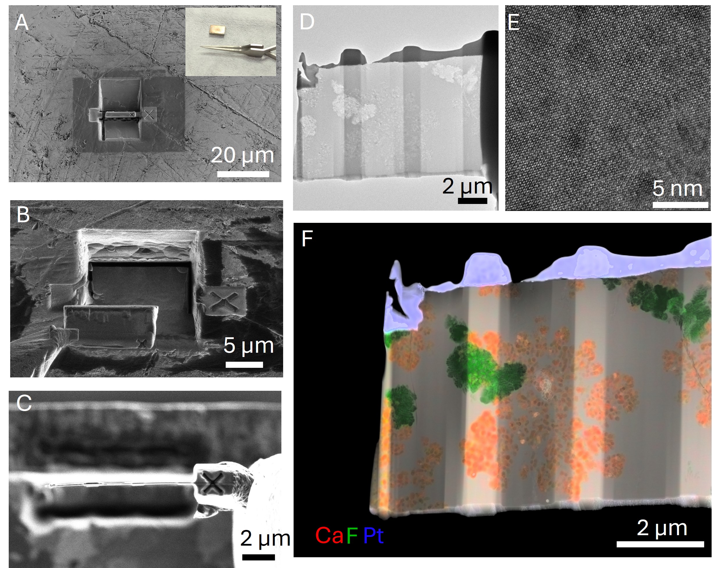
Visualizing the arrangement of atoms in a material provides invaluable insight into its bulk behavior. Properties such as conductivity, strength and stability originate from the atomic structure. Whether formed by a geological process or from a highly controlled processes in a clean room, accessing the atomic structure using transmission electron microscopy (TEM) requires incredibly thin samples that are polished with the utmost care. Classic preparation techniques could take a few days to a week. However, through improvement in automation, focused ion beam scanning electron microscopes (FIB-SEMs) have rapidly accelerated this process.
The Helios FIB-SEM in VINSE, is a powerful tool for imaging and manipulating matter at the nanoscale. Highly focused ions act as a nanoscale knife, allowing one to cut cross sections and mill patterns into practically any substrate all the while imaging with the electron beam. Paired with a tiny tungsten needle, one can cut-out cross sections and polish them down to less than 100 nm thick: making them suitable for atomic level imaging and elemental mapping with the Osiris TEM-STEM. Assisted with automation, one can prepare multiple samples and have time to image them in the TEM in the same day. Please contact James McBride for more information.