VINSE is excited to unveil the eleven winning images from our 2024 summer image competition. Since 2017, VINSE celebrates the work of our researchers, seeking images of materials or devices that have been fabricated, characterized or imaged using VINSE equipment with an annual image competition. Congratulations to this year’s winners. Each will receive a $250 cash prize and will have their art displayed in the Engineering Science Building.
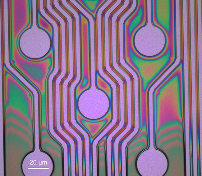
Microelectrode array patterned in photoresist
Fabricated and imaged in the VINSE facilities using the Karl Suss MA-6 Mask Aligner & Olympus Optical Microscope
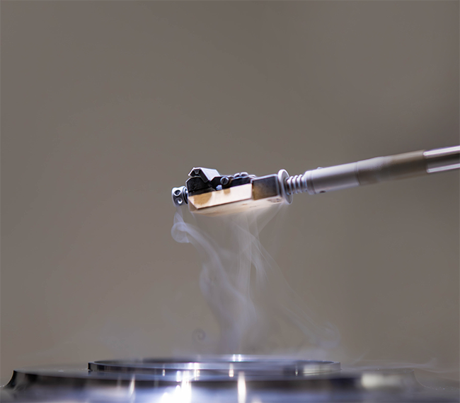
Liquid nitrogen preparation of biological samples for cryo-imaging using the FEI HeliosNanoLab G3CX in the VINSE Advanced Imaging Facility
Photograph taken using Sony A7 mirrorless camera, 85 mm
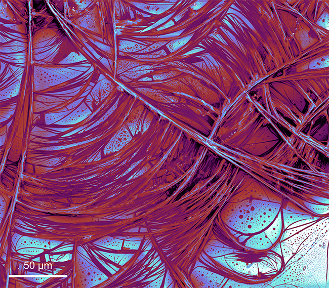
Rapid evaporation pattern of lead sulfide quantum dots that were suspended in chloroform
Imaged in the VINSE facilities using the Zeiss Merlin Scanning Electron Microscope
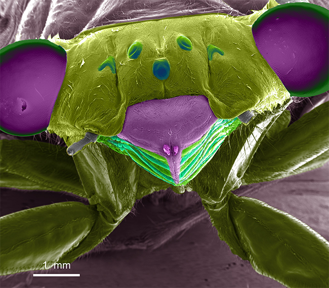
Brood XIX (13 year) Cicada carcass
Imaged by Dr. James McBride in the VINSE facilities using the Merlin Zeiss Scanning Electron Microscope
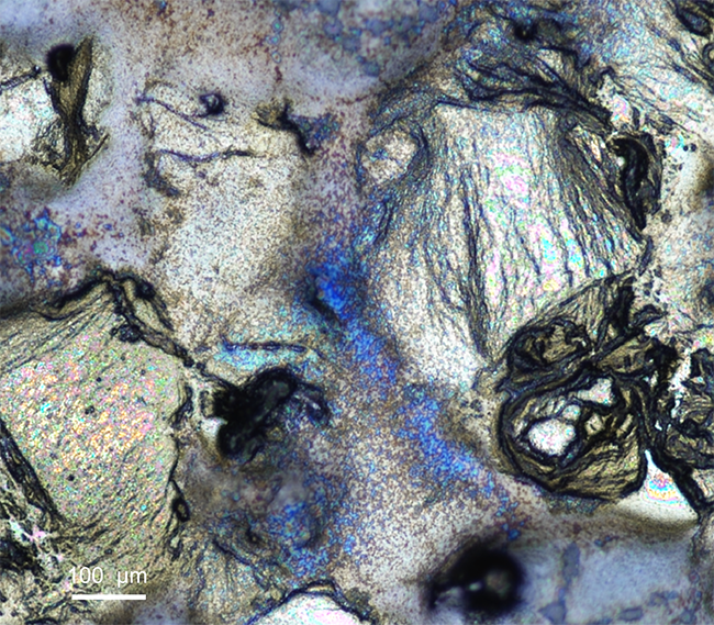
Mega-sonicated molybdenum disulfide (MoS2) flakes in IPA, drop casted on a SiO2/Si substrate
Imaged in the VINSE Facilities using the Bruker Atomic Force Microscope & the Olympus Optical Microscope
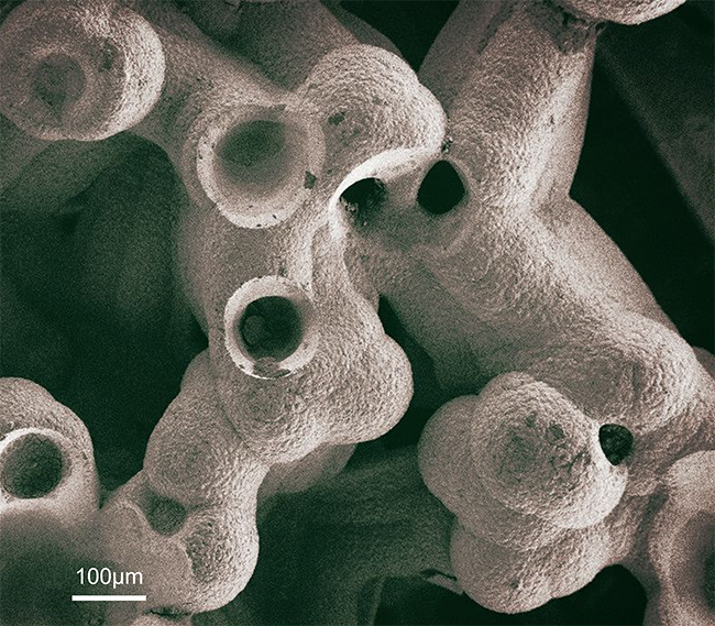
Deposition of Ni(OH)₂ on the surface of nickel foam through electroplating technology
Imaged in the VINSE facilities using the Zeiss Merlin Scanning Electron Microscope
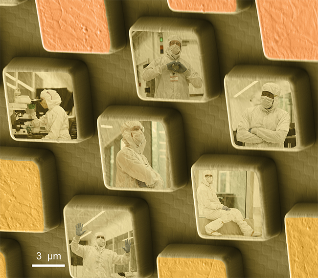
Surface and encapsulating layers of a photonic chip
Imaged in the VINSE facilities using the Merlin Zeiss Scanning Electron Microscope
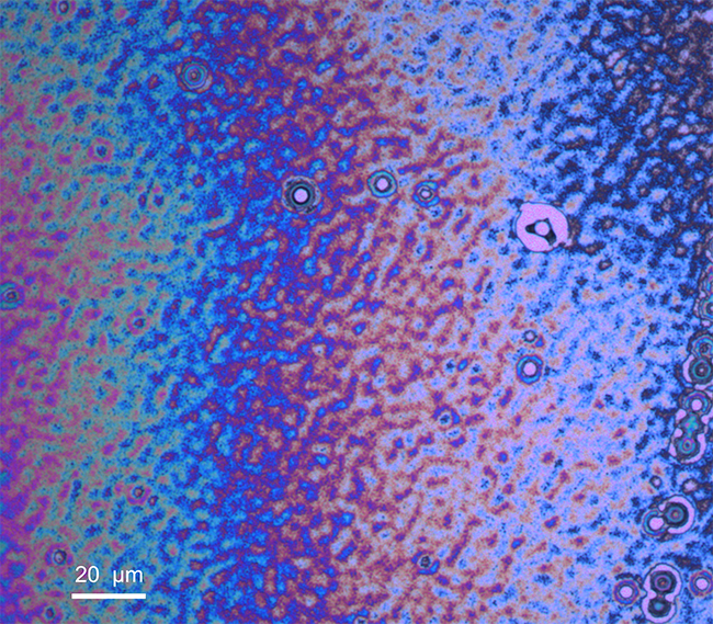
Etched perylene on silicon
Fabricated and imaged in the VINSE facilities using the Labcoter® 3 Parylene Deposition System, Oxford PlasmaPro 100 Cobra & the Olympus Optical Microscope
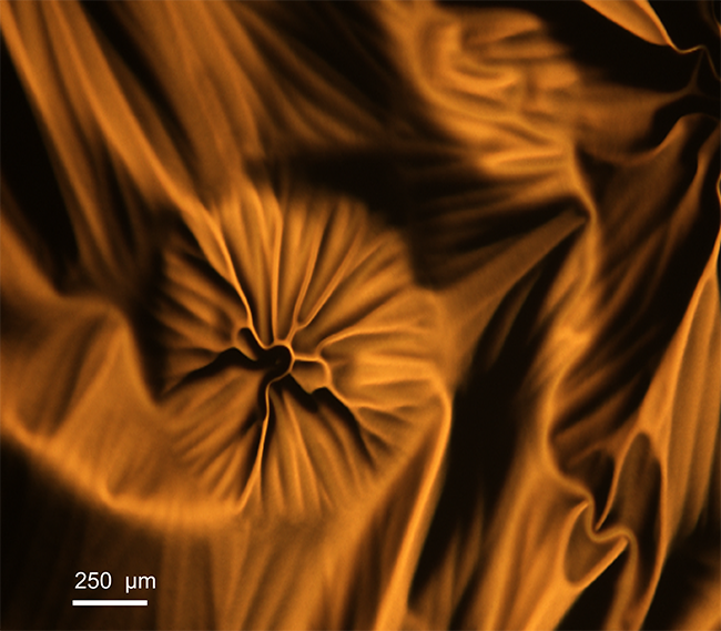
Electron beam evaporated gold film lifted off of Parylene-C coated Silicon wafer
Fabricated and imaged in the VINSE facilities using Karl Suss MA-6 Mask Aligner and Angstrom Engineering Amod Multimode Deposition System
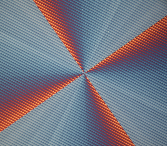
Patterned Resist on SiO2 on Si wafers
Imaged in the VINSE facilities using the Nikon Optical Microscope
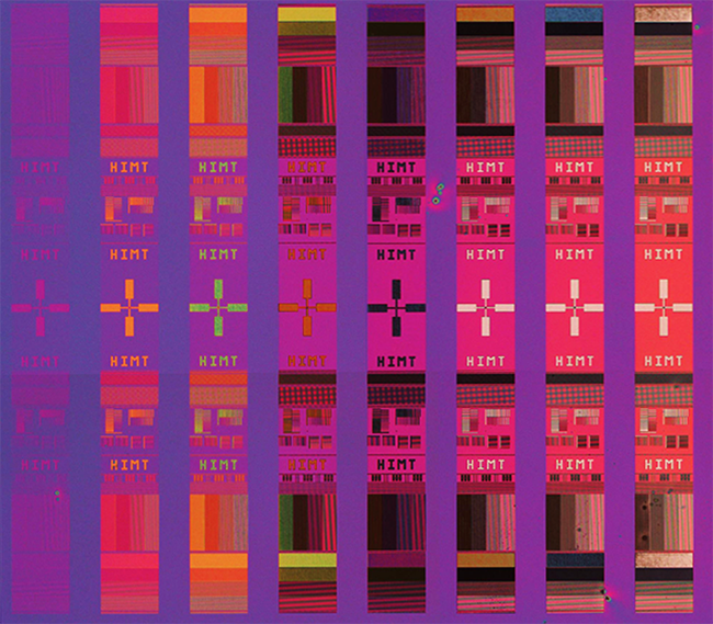
Photoresist patterned on a Si wafer using a range of different doses to find the ideal exposure parameters
Fabricated and imaged in VINSE using the Heidelberg Instruments uPG 101 Laser Writer and the Olympus Optical Microscope